Cadence Layout From Schematic

Dayna Schmidt III

Cadence spectre simulations performed Cadence tutorial Lvs layout schematic cadence calibre vs check simulation post

cadence analog circuits

cadence analog circuits

Design vlsi layout and schematic on cadence by ex_einstien_pal Layout of proposed detff all simulations are performed on cadence Cadence analog circuits

Schematic cadence layout skill devices binding creation between after community put capture

Circuit schematic in cadence design suiteCadence analog circuit tool circuits Ee5323 vlsi design i using cadenceCadence layout tutorial.

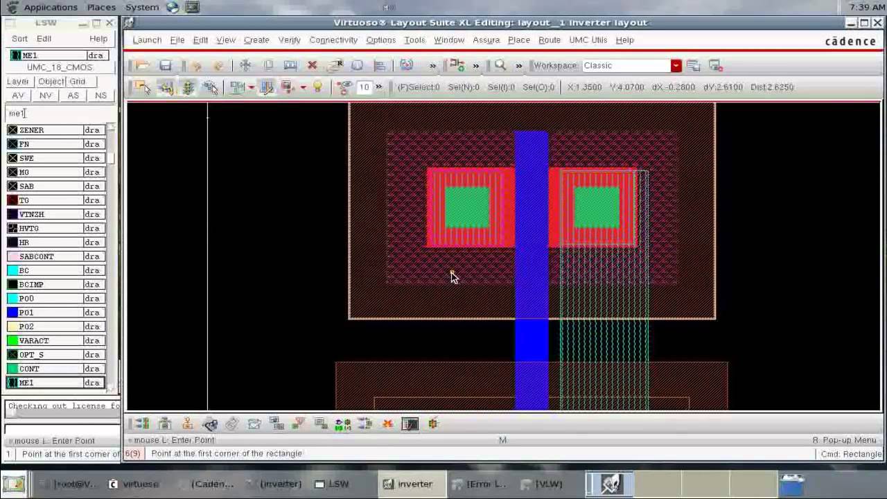
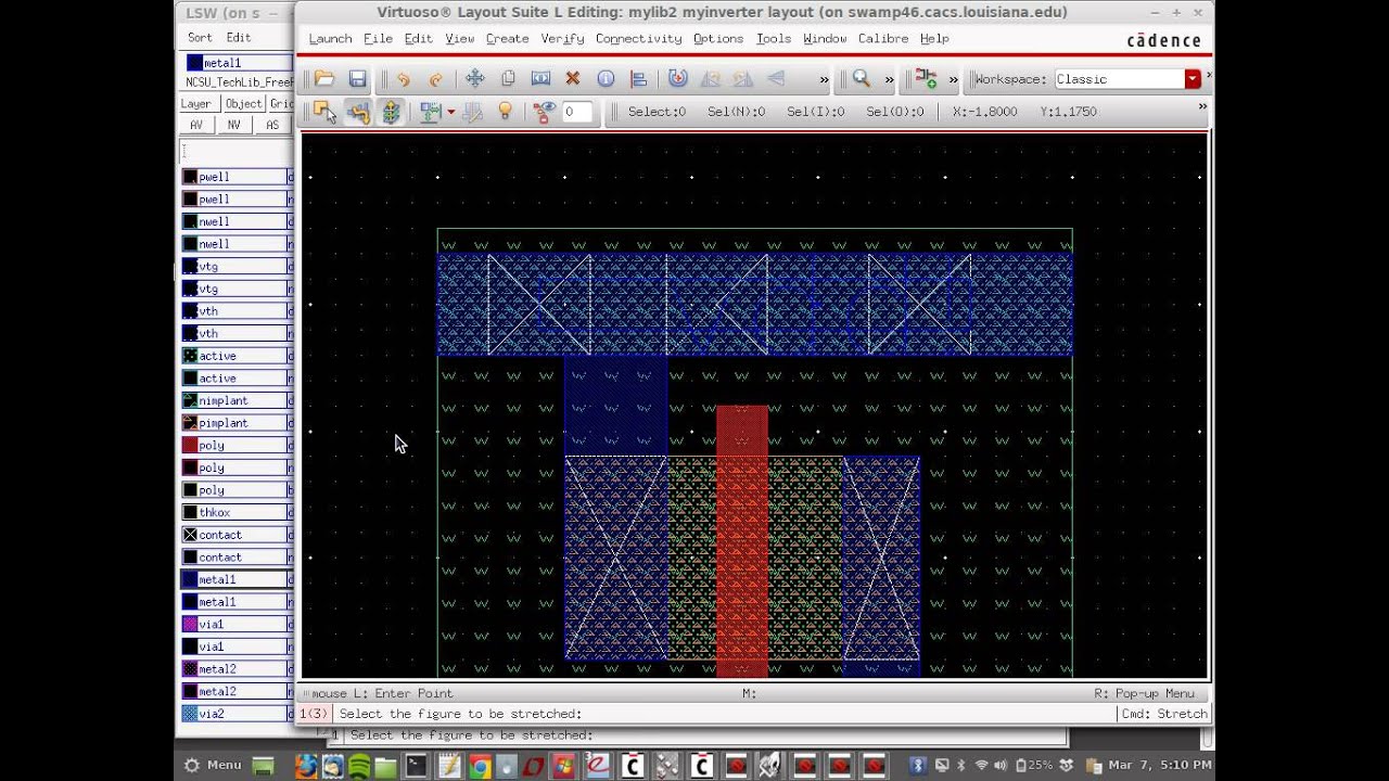
Cadence schematic suiteEe4321-vlsi circuits : cadence' virtuoso layout information Layout inverter cadence cmos tutorialLayout cadence inverter virtuoso vlsi inv cell create tutorial ece umn edu.

Layout of proposed DETFF All simulations are performed on Cadence

Layout cadence pmos virtuoso editor inv columbia edu should ee tutorials

Lvs (layout vs schematic)check in cadenceComparator cadence hysteresis cmos circuit schematic internal they representation schematics understandable maybe clear both same second output different just differential Comparator with hysteresis in cadenceLayout pin creation after binding the devices between schematic and.

Cadence layout tutorial (new)Vlsi cadence layout schematic fiverr screen .

Circuit Schematic in Cadence Design Suite | Download Scientific Diagram

Comparator with Hysteresis in Cadence

Cadence tutorial - CMOS Inverter Layout - YouTube

EE4321-VLSI CIRCUITS : Cadence' Virtuoso Layout Information

Design vlsi layout and schematic on cadence by Ex_einstien_pal | Fiverr

LVS (Layout vs Schematic)Check in Cadence | using Calibre | PEX | Post

layout pin creation after binding the devices between schematic and

cadence analog circuits

EE5323 VLSI Design I using Cadence

Cadence Layout Tutorial (new) - YouTube


YOU MIGHT ALSO LIKE